- Like
- SHARE
- Digg
- Del
- Tumblr
- VKontakte
- Flattr
- Buffer
- Love This
- Save
- Odnoklassniki
- Meneame
- Blogger
- Amazon
- Yahoo Mail
- Gmail
- AOL
- Newsvine
- HackerNews
- Evernote
- MySpace
- Mail.ru
- Viadeo
- Line
- Comments
- Yummly
- SMS
- Viber
- Telegram
- JOIN
- Skype
- Facebook Messenger
- Kakao
- LiveJournal
- Yammer
- Edgar
- Fintel
- Mix
- Instapaper
- Copy Link
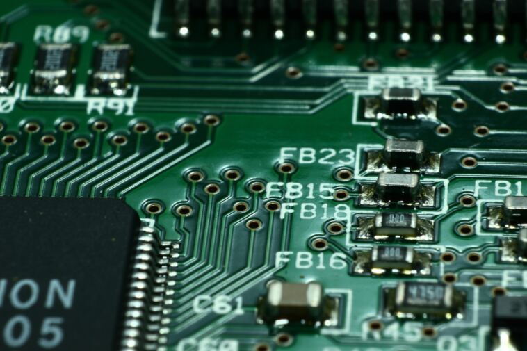
Printed Circuit Boards (PCBs) are the backbone of modern electronics, enabling the creation of intricate electronic devices we rely on daily. Beneath the metallic traces and components lies a crucial layer known as the solder mask. This layer serves a multitude of purposes, from protecting traces to preventing solder bridges.
In this article, we delve into the world of solder mask materials, their composition, properties, environmental aspects, and the exciting advancements shaping the future of PCB technology.
Solder Mask Materials and Functionality
The solder mask also referred to as the solder resist or solder stop mask, is a thin protective layer applied to the surface of a PCB. Its primary function is to insulate the copper traces and components from accidental solder bridging during the soldering process. The solder mask achieves this by providing a barrier between conductive areas and preventing the molten solder from flowing where it’s not intended.
Common materials used for solder masks include epoxy-based resins, liquid photo imageable solder masks (LPI), and dry film solder masks (DFSM). These materials are carefully formulated to provide excellent adhesion, thermal stability, and chemical resistance.
Polymer Composition in PCB Mask Materials
Epoxy resins are widely used in solder masks due to their excellent electrical insulation properties, adhesion to substrates, and resistance to various chemicals. These resins are often combined with additives like pigments to achieve the desired color. The formulation may also include fillers to improve the solder mask’s mechanical properties.
Liquid photoimageable solder masks (LPI) are polymers that can be applied as a liquid and then exposed to UV light through a photomask. This exposure hardens the areas that need to remain, while the unexposed portions are washed away. LPI solder masks offer high precision and are well-suited for intricate PCB designs.
Dry film solder masks (DFSM) consist of a thin polymer film with a tacky surface. The film is applied to the PCB and then laminated, with heat and pressure causing it to adhere. Once exposed to UV light through a photomask, the unexposed portions can be developed away, leaving the desired solder mask pattern. DFSM is advantageous for high-volume production.
Optical and UV Properties of Solder Mask Materials
Optical and UV properties play a crucial role in the application of solder masks. Most solder masks are designed to be opaque, preventing the passage of UV light. This opacity ensures that the UV light used in the photolithography process doesn’t penetrate the solder mask and affect the underlying components and traces.
However, some advancements have led to the development of solder masks with specific UV-transparency properties. These transparent solder masks enable the use of UV curing processes for components that are mounted on the opposite side of the board, enhancing overall production efficiency.
Environmental and Regulatory Aspects of PCB Mask Materials
In an era of increasing environmental consciousness, the impact of PCB materials cannot be ignored. Many PCB solder mask materials are now subject to stringent regulations aimed at reducing harmful substances. The RoHS (Restriction of Hazardous Substances) directive, for example, restricts the use of certain hazardous substances like lead, mercury, and cadmium in electronics manufacturing.
As a result, solder mask material manufacturers from pcba china are continually working to develop environmentally friendly options that comply with these regulations while maintaining the desired functional properties.
Advancements in Next-Generation PCB Mask Materials
The field of PCB technology is dynamic, with ongoing research and development leading to exciting advancements in solder mask materials.
Some of these advancements include:
Flexible and Stretchable Solder Masks: With the rise of flexible and wearable electronics, solder masks that can bend and stretch without cracking are becoming increasingly important. New materials are being explored to provide both protection and flexibility.
Conductive Solder Masks: In certain applications, having regions of a PCB act as low-resistance conductors can be beneficial. Conductive solder masks are being developed to allow controlled electrical connectivity in specific areas.
Self-Healing Solder Masks: Researchers are working on materials that can “self-heal” minor scratches or damage to the solder mask, prolonging the life and reliability of the PCB.
Enhanced Thermal Management: As electronic devices become more powerful, managing heat becomes crucial. Solder mask materials with improved thermal conductivity are being developed to help dissipate heat from critical areas of the PCB.
Nanotechnology Integration: Nanomaterials are finding their way into various aspects of electronics, and solder masks are no exception. Nanoparticles are being incorporated into solder mask formulations to enhance properties like adhesion, electrical insulation, and thermal conductivity.
Conclusion
The solder mask may be a seemingly minor layer in a PCB, but its role in ensuring proper functionality and reliability is paramount. As technology continues to evolve, so too will the materials and techniques used to create solder masks, shaping the future of electronics manufacturing. From eco-friendly formulations to cutting-edge functionalities, the world of solder mask materials is on a path of continuous innovation.

![the-6-stages-of-the-product-life-cycle-[+examples]](https://everythingflex.com/wp-content/uploads/2023/08/9093-the-6-stages-of-the-product-life-cycle-examples-150x150.webp-23keepprotocol)